
In almost every advanced technology like machine learning or artificial intelligence, one component that doesn’t seem to change is memory. The role that memory plays in the process of application development and network technologies is huge.
If we take a recent example, 5G connectivity for mobile devices is possible only when memory is processed at the endpoints of networks. The same can be said for many IoT projects that are in development.
Memory is undoubtedly going to help future AI inference engines. It will be one of the reasons for many successful modules of manufacturing and testing of device properties.
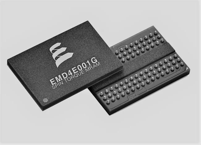
MRAM yields are distinct from any other semiconductor technology, and it is slowly replacing SRAM in various sectors. That is why it is a leading memory technology and is great for broad commercial availability.
Many people often think MRAM is made for all applications, but that is entirely misinterpreted because it needs fine-tuning and redesigns to target its intended purpose. If one wants to deploy a device with more endurance and speed, MRAM can be used by trading retention for higher endurance and speed.
The designers can make a huge impact by changing the critical magnetic tunnel junction (MTJ). They can achieve success in their respective target markets by finding a way to balance speed, endurance, and data retention. In this article, we will deep dive into some of the major aspects surrounding MRAM technology.
What is MRAM? (MRAM Meaning)
Magnetic RAM or Magneto-resistive RAM is a new form of random access memory, and the technological changes made it non-volatile. When we hear non-volatile electronic components, it only means one thing- data retention.
Yes, it can store data and retain information. The only difference we observe between MRAM and ordinary RAM is magnetic charges instead of electric. It makes the MRAM more advantageous to the designers of mobile and other computing devices because they do not need a constant flow of power to retain data.
As a result, the production cost for this technology is significantly low compared to other memory technologies. Speed is also a crucial factor in MRAM, as it is faster than every other technology that includes FLASH and EEPROM.
Even though this robust and high-level technology has been around for a better part of the last decade, it is only now that the manufacturing is taking place in large volumes.
How does MRAM Work?
When it comes to MRAM's functionality, it is different from DRAM and follows some quantum phenomenon in the process. MRAM does not use electric charges to verify if the incoming light pulses contain one or zero; it uses a metal plate made of ferromagnetic material.
There is a thin lining separating both plates, and that acts as an insulation layer. Now, MRAM determines the binary value by considering the orientation of magnetic fields. One of the ferromagnetic plates remains magnetized from the start, and the other can or cannot be magnetized at any instant.
The structure consisting of ferromagnetic plates and an insulation layer is called magnetic tunnel junction(MJT). We mentioned this before, and we said that it could have a huge impact on the overall MRAM functionality.
The basic structure, MJT, works on a quantum phenomenon called electron tunnelling. It simply means that electrons from the plate will migrate to the opposite plate and do that using an insulation layer. As the thickness is low with the insulation layer, electrons easily find their way to the other plate. The determining factor for this process to occur at a high level is plate orientation. If the plates are oriented in a parallel fashion, then electron tunnelling occurs, and we can observe a change in the junction's electrical resistance. This change will finally let us know if the binary bit is one or zero.
Another important point to highlight is that MRAM can withstand wear and tear. Unlike flash memory, it doesn't degrade without the physical mass being damaged.
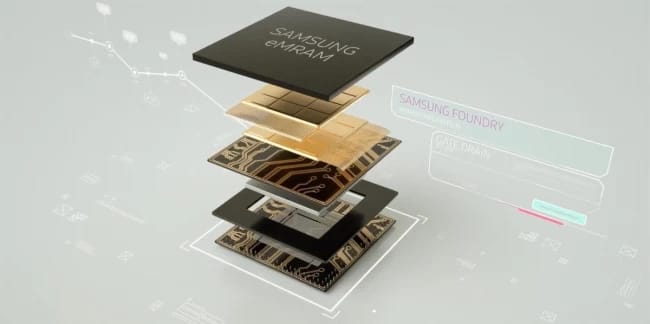
MRAM Design & Creation
It has taken close to ten years to manufacture MRAM in large volumes, and the main reason it took so long is that no one could find a structure or design that allows simple fabrication. To obtain the optimum MRAM structure, manufacturers tried out many designs and materials. Still, nothing seemed to work out at that time. One such early-phase design was done using eight different shadow masks made out of metal, and all of them were computer-controlled. Currently, the design involves a thin Aluminium layer, and manufacturers are using the in-situ plasma oxidation method to form the tunnel barrier. This structure finally made everyone feel satisfied because the changes in the levels of resistance were seen.
Main Characteristics of MRAM
The characteristics for any non-volatile memory remain the same, and they are: read speed, write speed, data retention, and endurance, These four will not change for any non-volatile memory technology, and they are essential to know for designers to design the MJT and surrounding circuits.
The four parameters are important for that reason and for determining the current required and stability of the circuit when it faces thermal fluctuations or some other disturbance. The characteristics of MRAM help in many ways to achieve total optimization of an MJT design.
Let's look at each characteristic and understand how they contribute to achieving optimum structure for MRAM technology.
MRAM Write Speed

In MRAM, writing is not a simple process, and it requires many things to go right. The main idea surrounding the working of MRAM is the torque of the electron being transferred to the free layer. Even though it's a continuous process, it still requires a couple of electrons to get started.
As it depends on the deviation coming from the thermal fluctuations, the initiation of writing on MRAM varies each time it's programmed. The initiation rate will determine how much time it will take for the device to switch. It cannot be predicted because, inside the system, some bits can be written and programmed faster than others.
If it is a repeated set, then we can expect better initiation rates. Another way to help with the writing is to use certain materials to make the device thermally unstable. One can also engage in magnetic damping to make the device fluctuate on its own. The thing with write speed is that if it gets too high, the MJT will experience a lot of wear and tear.
It is mainly the case for STT MRAM. If you are using SOT MRAM technology, you need not worry about the device's endurance because the current doesn't go through MTJ, and it passes through a different path that is parallel to the layers.
MRAM Read Speed

Read speed is not similar to write speed because the way it is controlled is entirely different. The two main factors that increase or decrease the read speed are magnetoresistance and memory window. If the zero and one states of the memory are wide apart and the polarization is higher than usual, then reading MRAM becomes easy.
If the sense amplifier can quickly incorporate the current into the circuit, then the read speed will be higher. Even in the case of reading speed, there are some limitations to follow. Read speed can act as write speed if the incoming current is higher than the standard limit. Unlike write speed, the read speed will not change for SOT MRAM, and it will behave similarly to write speed if the current is not managed correctly.
Endurance
Whenever the electrons make their way out of the tunnel to reach the opposing plate, it contributes to the thin insulation layer's wear. The same can be said about flash memory too. When this process happens multiple times, it is called an overriding effect. It brings a significant risk of complete breakdown.
The phenomenon that occurs during overwriting is called time-dependent dielectric breakdown, or TDDB. As this is a voltage-dependent effect, we can make adjustments to lower the voltage and increase a device's lifetime. In simple terms, lower voltages mean higher endurance for MRAM technology.
Data Retention

One major factor dominating the level of data retention on MRAM technology is the energy barrier. The best thing about MRAM in terms of data retention is that it can be configured for ten seconds, minutes, or even years.
MRAM data retention used to be a big challenge in the early days of development because it used not to handle reflow cycles. The temperatures could go up to 260 degrees, and it was difficult for the device to stay stable for a long time.
So, temperature stability is crucial to consider if you want to retain data even after the power is lost. The other factors influencing data retention are magnetic field and anisotropy fields.
How can MRAM help develop Edge Computing?
When we talk about edge computing, it is not only limited to the Internet of Things(IoT), but there are many other applications in fields like medicine, robotics, and artificial intelligence. All these categories of applications coming under edge computing can benefit from using MRAM.
It is beneficial for every edge computing device because they want high-speed, low-latency, and cost-effective memory. While there are other alternatives available in the marketplace, everyone goes with MRAM technology only. It happens because, in other memory technologies, we need to trade-off in multiple areas. So if you have endurance, you might not get speed and data retention.
The only optimal choice for designers is to go with MRAM technology. The leakage is also low with MRAM, and the write cycle count is high, so in every MRAM technology area, designers get optimal conditions for advancing edge computing.
Use-Cases & Target Application for MRAM Technology
MRAM technology mainly has four target applications highlighting different areas and device requirements. The complexity to achieve perfection in each application increases from stand-alone memory to last-level cache. The first application deals with devices that are focusing on battery-backed SRAM and DRAM. Some also use hard drives. The next in the line is embedded MRAM, and it is more focused on SoCs.
In this application, MRAM takes over the system chip and replaces NOR flash memory. It is important to note that MRAM can't take over the NAND flash position. That would require a robust, economic integration with the help of CMOS.
The third and fourth applications focus only on SRAM. The mobile cache and last level cache help in achieving low power. In the mobile cache, we get to see a proper unification of SRAM and flash memory. As it is stored in a small MRAM block, it is limited to only portable or small IoT devices. Coming to the last application, the last level cache, is still not achieved because the performance requirements are high. It is not available or in use right now, but we can expect its arrival in a couple of years.
The use cases for MRAM technology mainly persist in the IoT and AI space. A use-case that is seen every day using MRAM is data logging. We see RFID tags in hospitals scanning employees' data and logging the same in a different device. People responsible for data logging use a minimum of two megabits of MRAM to secure long-term data accumulation.
A use-case implementing MRAM technology's speed belongs to edge devices that scan the data and identify patterns. This operation requires high processing speed, and MRAM meets the demands in every way.
The final use case implementing MRAM technology belongs to healthcare devices. These devices need high endurance as it is used in a hospital environment. They also require a technology that is immune to radiation. MRAM meets both the demands and the RFIDs help in a great way to monitor consumables and identify medical equipment.
Conclusion
MRAM technology is soon going to take over many manufacturing units to reduce total power consumption. Power is a crucial parameter for designing, and MRAM makes it easy to integrate into any specific application design. The four characteristics can be balanced in any scenario, and we will not require to trade off any area to increase overall performance.
There is more room for improvement in MRAM, and other memory technologies lack additional energy savings. MRAM provided that by using a power gating system architecture. The power is more, and the speed is more, the endurance is more. Hence, MRAM technology is more reliable than conventional memory technologies.

I'm fascinated by the IT world and how the 1's and 0's work. While I venture into the world of Technology, I try to share what I know in the simplest way with you. Not a fan of coffee, a travel addict, and a self-accredited 'master chef'.